
Bubbles and Anti-Hedgehogs: Studying the Nanostructures That Could Lead to the Future of Data Storage
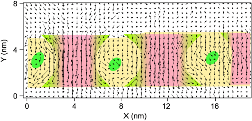
Image of some of the nanostructures that physics researchers say could be used to store data.
Electronic devices are getting smaller, faster and more efficient, but these improvements are limited by the size of their components — the transistors, resistors, capacitors and other components that are crammed onto smaller and smaller integrated circuits.
In order to overcome this challenge, physicists are exploring a new method of storing and transmitting electrical current and information: using the complex structures of certain crystalline materials, referred to as “ferroelectric” or “ferromagnetic.” At the nanoscale, “ferroelectric” materials exhibit ordered patterns of electric dipoles. Electric dipoles are pairs of positive and negative charges that are caused by atomic displacement — atoms that have moved from the “ideal” position dictated by the crystalline lattice. Ferromagnetic materials exhibit similar patterns caused by a characteristic called spin.
These patterns can sometimes feature complex objects. Certain types of objects, called topological defects, are stable enough to withstand the wear and tear faced by electronic devices, and researchers can move them or alter their properties by applying an electric field. What if, physicists ask, these patterns could store and transmit information as reconfigurable elements of an integrated circuit?
Researchers in Laurent Bellaiche’s physics group at the University of Arkansas work with colleagues around the globe to study these materials, using state-of-the-art experimental techniques and computer simulations. In a previous study, they used computer modeling to demonstrate that domain walls, or boundaries that separate different perfectly ordered regions in ferroic materials, could transfer electric charge through a type of electrical current called displacement current.
Now, Bellaiche and colleagues Yousra Nahas and Sergei Prokhorenko are working with a team that includes physicists from China and Germany. With grants from Defense Advanced Research Projects Agency (DARPA) and the Army Research Office, this team is the first to observe certain topological defects in ferroelectric materials. Theoretically, these structures could be configured and manipulated individually by an electric field, or by using changes in temperature and pressure, which means they could be used to encode data.
In a paper published in Physical Review Letters, the researchers described the structures, which they observed through high-resolution scanning transmission electron microscopy and simulated at the U of A High Performance Computing Center.
As Nahas and Prokhorenko explained, having both experimental observations and computer simulations is important because these two methods not only validate but also complement each other. “The observation proves the model is accurate,” said Nahas, “but also, the model can provide microscopic understanding to reality itself.”
Prokhorenko added, “Sometimes it’s hard to identify the main factors leading to a certain observation. Simulations allow us to construct a simplified model of reality, and eliminate factors one after the other to understand why it happens. They can also help prove that the obtained result is robust and reproducible.”
The researchers observed several different kinds of structures, which they then simulated to study and characterize further. The structures are formed by variations in the orientation of the dipoles, which are illustrated with arrows in the images below. The simulations were performed at the Arkansas High Performance Computing Center, which is funded through multiple National Science Foundation grants and the Arkansas Economic Development Commission.
MICROSCOPY IMAGE AND DATA


VORTICES

DISCLINATIONS


WAVES AND BUBBLES


HEDGEHOGS AND ANTI-HEDGEHOGS

This story originally appeared in the University of Arkansas’ Newswire publication. Please visit news.uark.edu for more stories like this.
Camilla Shumaker
Director of Science and Research Communication, University Relations
479-575-7422 // camillas@uark.edu